-
Highlight
Buried Vias 2 Layers PCB
,Blind 2 Layers PCB
,1.6mm pcb and assembly
-
Min Trace/Space4/4mil
-
Board Thickness1.6mm
-
Solder Mask ColorGreen
-
Copper Thickness1oz
-
Layer Number2
-
MaterialFR4
-
Blind/Buried ViasYes
-
Impedance ControlYes
-
Place of OriginGuangdong, China
-
Brand NameKZX
-
Certification25020001470ROS
-
Model NumberKZX2023120512
-
Minimum Order Quantity10 piece
-
PricePrice negotiation
-
Packaging DetailsCustomer specified packing
-
Delivery TimeSubject to order status
-
Payment TermsT/T, L/C,Paypal,western union etc
-
Supply Ability3 PCB SMT lines
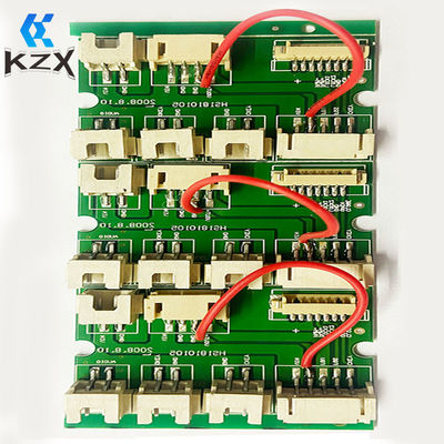
Blind Buried Vias 2 Layers PCB With Green Solder Mask Integration
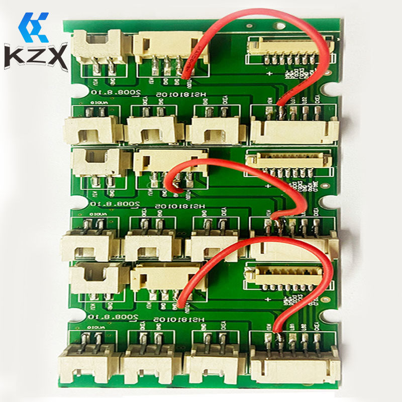
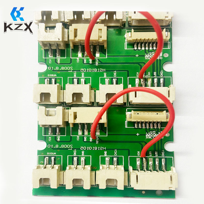
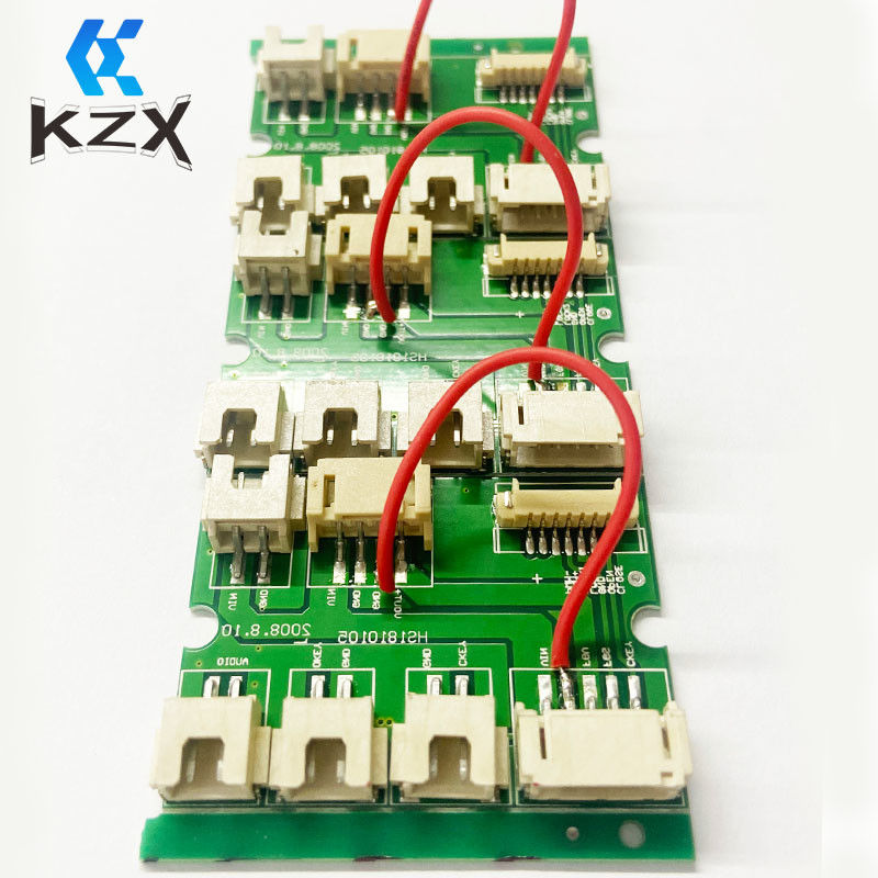
Blind/Buried Vias 2 Layers PCB With Green Solder Mask Integration
Product Description:
2 Layers PCB is a communication type of printed circuit board (PCB) with double-sided construction, featuring a total thickness of 1.6 mm and a material of FR4. It is designed for advanced applications with 4/4mil minimum trace/space, impedance control and blind/buried vias for better connectivity. It is a reliable double-sided PCB board with high-density components and high-speed digital signal transmission capability, ideal for a wide variety of communication applications.
Features:
- Product Name: 2 Layers PCB
- Blind/Buried Vias: Yes
- Board Thickness: 1.6mm
- Material: FR4
- Solder Mask Color: Green
- Min Trace/Space: 4/4mil
- Communication PCB: Yes
- FR4 Multilayer PCB: Yes
Technical Parameters:
| Parameter | Value |
|---|---|
| FR4 Multilayer PCB | Yes |
| Double Sided PCB Assembly | Yes |
| Double Sided PCB Board | Yes |
| Min Trace/Space | 4/4mil |
| Blind/Buried Vias | Yes |
| Board Thickness | 1.6mm |
| Material | FR4 |
| Impedance Control | Yes |
| Layer Number | 2 |
| Solder Mask Color | Green |
| Copper Thickness | 1oz |
Applications:
KZX 2 Layers PCB is a great choice for applications such as FR4 Multilayer PCB, Heater PCB, Double Sided PCB Board and Two Layers PCB. It offers a superior combination of performance, quality and cost-efficiency. Its model number is KZX2023120512 and its place of origin is Guangdong, China. It has passed strict certification with the certification number 25020001470ROS. With minimum order quantity of 10 pieces, price can be negotiated and it is packed according to customers' requirements. With 3 PCB SMT lines, the delivery time is subject to order status and payment terms T/T, L/C, Paypal, western union etc. are available. The material used is FR4, with 4/4mil minimum trace/space and impedance control. It also supports blind/buried vias.
Customization:
We provide 2 Layers PCB customization service for our clients with best quality and reasonable price.
Brand Name: KZX
Model Number: KZX2023120512
Place of Origin: Guangdong, China
Certification: 25020001470ROS
Minimum Order Quantity: 10 piece
Price: Price negotiation
Packaging Details: Customer specified packing
Delivery Time: Subject to order status
Payment Terms: T/T, L/C,Paypal,western union etc
Supply Ability: 3 PCB SMT lines
Min Trace/Space: 4/4mil
Layer Number: 2
Board Thickness: 1.6mm
Solder Mask Color: Green
Impedance Control: Yes
Advantages: Our 2 Layers PCB can provide great performance for communication products with features such as high reliability, low cost, high quality, fast delivery, and good after-sales service.
Application: Our 2 Layers PCB are widely used in communication products such as mobile phones, computers, routers, and other communication products.
Support and Services:
2 Layers PCB provides technical support and services to all of our customers. Our team of experienced engineers and technicians are available to assist you with any questions or issues you may have regarding our products.
We offer telephone and email support, as well as online tutorials and FAQs. If you require more in-depth assistance, our team is also available for on-site visits to help you troubleshoot any problems you may have.
In addition, we offer a variety of services to ensure that your PCBs are designed and manufactured to the highest quality standards. We provide consulting services to help you select the best components and materials for your PCBs, and our team can also help you optimize your design for maximum performance.
We are committed to providing excellent customer service and technical support, and we strive to ensure that our products meet all your needs. If you have any questions or concerns, please do not hesitate to contact us.
Packing and Shipping:
2 Layers PCB will be packaged and shipped following the following procedures:
- The product will be placed in a static-free bag and sealed.
- The PCB will then be placed in a specialized cardboard box.
- The box will be packaged with specialized bubble wrap.
- The package will then be shipped by a reliable courier.
Our products are sold all over the world, you can rest assured.