
-
Highlight
Green Solder Mask 2 layer pcb board
,2 layer pcb board Electronics
,1.6mm 2 sided pcb
-
Blind/Buried ViasYes
-
MaterialFR4
-
Min Trace/Space4/4mil
-
Board Thickness1.6mm
-
Impedance ControlYes
-
Layer Number2
-
Solder Mask ColorGreen
-
Copper Thickness1oz
-
Place of OriginGuangdong, China
-
Brand NameKZX
-
Certification25020001470ROS
-
Model NumberKZX2023120512
-
Minimum Order Quantity10 piece
-
PricePrice negotiation
-
Packaging DetailsCustomer specified packing
-
Delivery TimeSubject to order status
-
Payment TermsT/T, L/C,Paypal,western union etc
-
Supply Ability3 PCB SMT lines
Green Solder Mask 2 Layer PCB Board For Electronics 1.6mm
Green Solder Mask 2 Layers PCB Board For Electronics - 1.6mm Thickness B2B
Product Description:
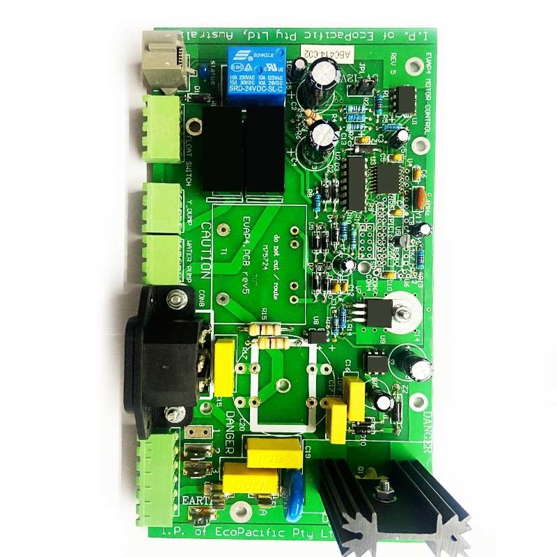
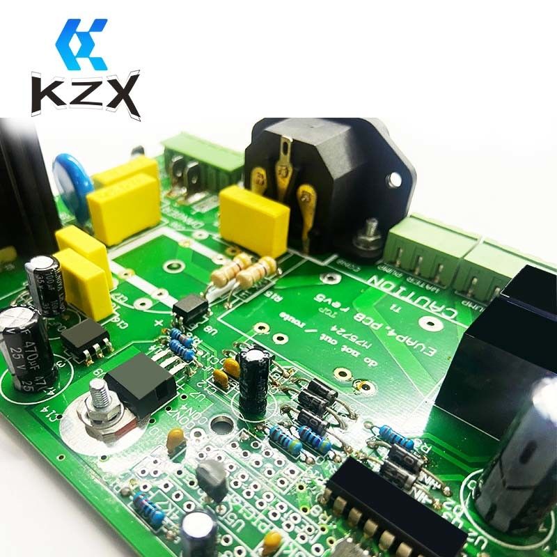
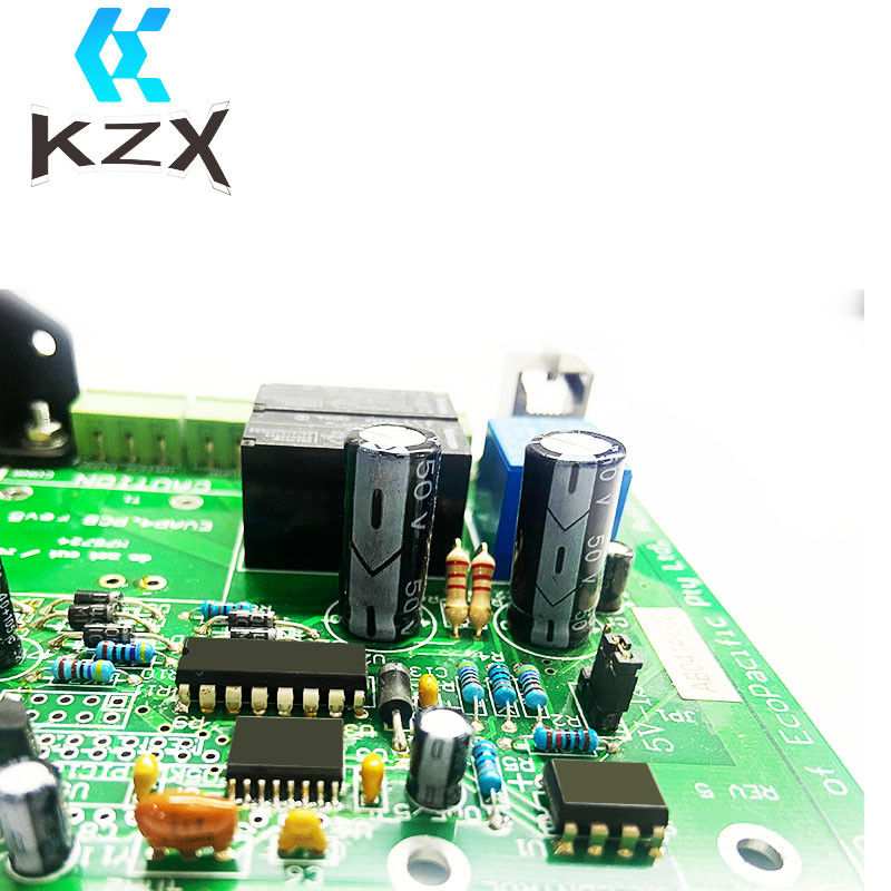
2 Layers PCB is custom designed to meet the needs of your application. It is constructed using high quality FR4 material which provides superior strength and durability. It is designed with a two-layer stackup, enabling you to achieve excellent impedance control. The board has solder mask in green color and blind/buried vias to ensure complete traceability and long-term reliability. It is ideal for use in harsh environments and high temperature applications, such as heater PCBs.
Features:
- Product Name: 2 Layers PCB
- Copper Thickness: 1oz
- Layer Number: 2
- Board Thickness: 1.6mm
- Blind/Buried Vias: Yes
- Material: FR4
- Specialty: Communication PCB, Double Sided PCB Board, Communication PCB Board
Technical Parameters:
| Parameter | Value |
|---|---|
| Blind/Buried Vias | Yes |
| Material | FR4 |
| Min Trace/Space | 4/4mil |
| Impedance Control | Yes |
| Solder Mask Color | Green |
| Layer Number | 2 |
| Board Thickness | 1.6mm |
| Copper Thickness | 1oz |
| PCB Assembly | Double Sided |
| PCB Type | Communication PCB |
| PCB Material | FR4 Multilayer |
Applications:
KZX 2 Layers PCB is a great choice for communication, double sided PCB assembly, and custom PCB boards. With its model number KZX2023120512, this board is certifed with 25020001470ROS and has a minimum order quantity of 10 pieces. The price is open for negotiation and packaging details can be customized according to customer needs. The estimated delivery time is subject to order status, and the payment terms include T/T, L/C, Paypal, and Western Union. KZX 2 Layers PCB also has a strong supply ability with 3 PCB SMT lines. Its min trace/space is 4/4mil, board thickness is 1.6mm, and the blind/buried vias are both available. It also has a solder mask color of green and copper thickness of 1oz. Hence, KZX 2 Layers PCB is a great choice for your communication, double sided PCB assembly, and custom PCB boards needs.
Customization:
Brand Name: KZX
Model Number: KZX2023120512
Place of Origin: Guangdong, China
Certification: 25020001470ROS
Minimum Order Quantity: 10 piece
Price: Price negotiation
Packaging Details: Customer specified packing
Delivery Time: Subject to order status
Payment Terms: T/T, L/C,Paypal,western union etc
Supply Ability: 3 PCB SMT lines
Material: FR4
Board Thickness: 1.6mm
Min Trace/Space: 4/4mil
Copper Thickness: 1oz
Blind/Buried Vias: Yes
KZX offers custom 2 Layers PCB service for communication, FR4 multilayer and double sided PCB assembly.
The PCB is made of high-quality FR4 material with a thickness of 1.6mm, copper thickness of 1oz, and min trace/space of 4/4mil.
It also supports Blind/Buried Vias and other advanced technologies.
Support and Services:
2 Layers PCB technical support and service provides customers with a range of services, including:
- Design and development of 2 layers PCBs
- Manufacturing and testing of 2 layers PCBs
- Troubleshooting and repair of 2 layers PCBs
- Technical advice and guidance on 2 layers PCBs
- Software and firmware updates for 2 layers PCBs
- Training and educational resources for 2 layers PCBs
- Replacement parts and components for 2 layers PCBs
Packing and Shipping:
Packaging and Shipping for 2 Layers PCB:
The 2 Layers PCB will be securely packaged in antistatic bagging and bubble wrap. It will then be placed in an appropriate sized box filled with cushioning for transport. The box will be securely sealed with strong adhesive tape and labeled with the appropriate shipping address. All shipments will be tracked and insured to ensure safe and timely delivery.
Our products are sold all over the world, you can rest assured.